
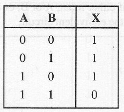
The output is high only IF the inputs (A and B) ate not in the high logic level. The symbol and the equivalent circuit is shown in figura 1.

Figure 1
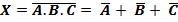
Equation 1
2-Input NAND Gate

Where:
X is the input logic level
A and B are the output logic levels
Truth Table – 2-Input NAND gate
Equation 2
3-Input NAND Gate
Equation 2
Where:
X is the input logic level
A, B and C are the output logic levels


