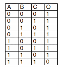
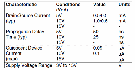
Description: Each of the three 8-Input NAND gates found in this package oan be used independently.

Pin Names:
Vdd - Positive Supply Voltage [BV to 15V]
Vss - Ground
A1, B1, C1, A2, B2, C2, A3, B3, C3 - Inputs
Q1, Q2, Q3 – Outputs

Operation Mode.
Logic levels are applied to the inputs resulting in a logic level at the output as shown by the truth table.

Applications:
Logic Functions
Oscillators
Digital Amplifiers
Observations:
The device can be used as a triple 2-Input NAND gate if one of the inputs of each gate remains at the “'1” logic level.


