
Description: This device is formed by two independent NOR gates and an inverter.
Functional Diagram and/ or Package:
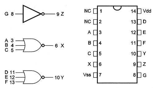
Pin Names
Vdd - Positive supply voltage [3 V to 15 V]
Vss - Ground
A, B, C, D, F, G, H - Inputs
X, Y, Z – Outputs
Operation Mode:
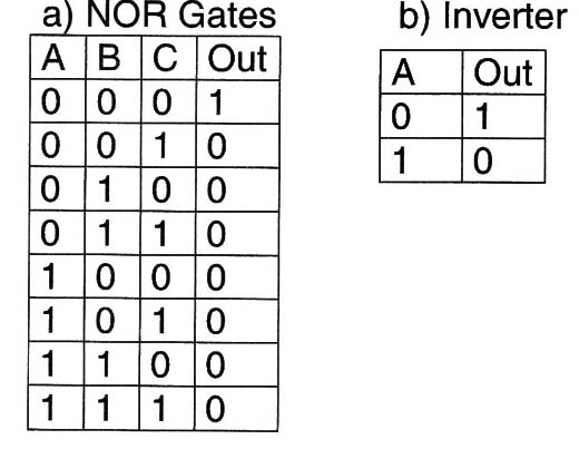
The logic signals are applied to the inputs of the gates and the resulted logic levels are taken from the outputs. See the truth table for more details.
Electrical Characteristics

Other Devices:
3-lnput NOR Gates: 4023, 4025 [buffered]. Inverters: 4009 [buffer], 4049 [buffer], 4069
Applications: NOR gates and the inverter can be used in their basic functions adding logic to a project, such as in oscillators, driving stages, and digital amplifiers.
Observations: This device is not recommended for new projects since its functions can be found in other devices of the same family. It is not always easy to find.


