
Description: This device is formed by four 2-input independent NOR gates in the same package.

Functional Diagram or/and Package:
Pin Names:
Vdd - Positive Supply Voltage [3 V to 15 V]
Vss - Ground
A1, B1, A2, B2, A3, B3, A4, B4 - Inputs
X1, X2, X3 - Outputs
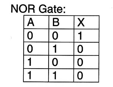
Truth Table:
Operation Mode:
The logic signals are applied to the inputs and the resulting logic level appears in the output of each gate.
Electrical Characteristics:

Applications: In addition to use as a logic block, the 4001 can also be used in oscillators, buffers, and time delay applications.
Observations:
OR gates and inverters can be associated to perform as a NOR gate.
If the inputs are tied together the logic gates will operate as inverters.


