
ART2278S ART2309
What can be done with an operational amplifier? In fact, there is no limit to this, and in the case of both amateur and professional electronics, we can find a multitude of projects. Most of these projects are based on the best known of all operational amplifiers, the 741. Based also on this amplifier, in this article we will give some theory about the so-called voltage comparators and window discriminators, which are configurations with very important applications in both professional and amateur electronics.
We will complete the article with some immediate diagrams that, without a doubt, can serve as a basis for more complex projects. We begin our explanations with the analysis of the 741 IC itself.
1. Operational Amplifiers
Figure 1 shows the symbol adopted to represent an operational amplifier.
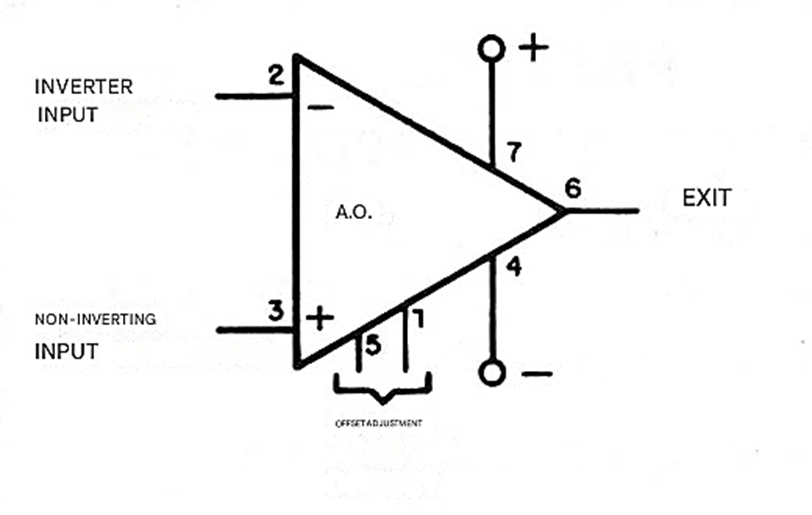
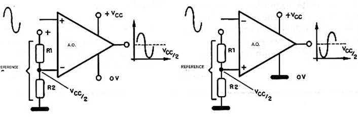
As we can see, it has two inputs: an inverting input, marked with (-), and a non-inverting input, marked with (+). The output is unique and, as additional elements, we have the power supply terminals and, possibly, the external compensation and leakage current adjustment (offset) terminals. If we apply a signal to the non-inverting input, it will be amplified and will appear with the same phase at the output. If the signal is applied to the inverting input, it will be amplified and will appear at the output with the phase inverted. Figure 2 shows what happens with a sinusoidal signal.
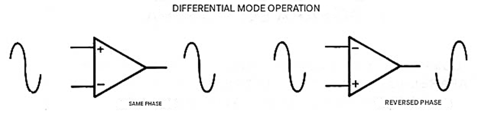
The signal can also be applied between the inputs, which means that we apply a differential voltage that will be amplified according to its polarity. This means that it amplifies the voltage difference between the inputs. If this difference is positive, we have a positive output, and if the difference is negative, we have a negative output (Figure 3).
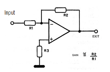
An ideal operational amplifier has infinite input resistance, infinite voltage gain, and zero output resistance. In practice, we do not achieve these results: the input impedance is high, about M ohms, the output impedance is low, about tens of ohms, and the gain can vary between 5,000 and 200,000 for the most common types. We can control the gain of an operational amplifier through negative feedback, as shown in Figure 4.
2. The 741 IC
The 741 can be found commercially with designations that depend on the manufacturer, such as LM741, MC1741, SN72741, uA741, etc., and is one of the most popular and versatile operational amplifiers. In our country, it can be found very easily, as it is imported by many distribution companies. Figure 5 shows its casing with terminal identification and the equivalent internal circuit.
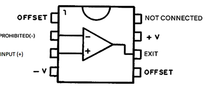
The characteristics of this integrated circuit are:
• Maximum supply voltage (symmetrical source): 18 - 0 - 18 V
• Maximum power dissipation: 670 Mw
• Input offset voltage (typ.): 0.8 mV
• Input impedance (min.): 1 M ohms
• Operating range (typ.): 1 MHz
• Gain (typ.): 200,000
• CMRR (typ.): 95 dB
• Output resistance: 75 ohms
3. Voltage Comparators
One of the interesting applications for operational amplifiers is the voltage comparator. The first type is shown in Figure 6, and the operating principle is described below.
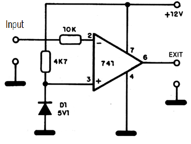
We fix the reference voltage at the non-inverting input using a zener diode. In our case, this voltage is 5.1 V given by a 400 mW zener diode. Thus, when we apply a voltage to the input, the operational amplifier amplifies it, comparing it to the reference voltage. Since the amplifier's gain is very high, a voltage difference of only a few millivolts between the two inputs will be enough to cause saturation at the output, that is, to obtain values close to zero or the positive supply voltage. If the input voltage is lower than the reference voltage, we have its amplification with phase inversion, resulting in a positive voltage close to the supply voltage. This is section 1 of the graph shown in Fig. 7.
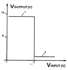
However, when the input voltage exceeds the reference voltage, we will have a positive difference in values which, after amplification with the inverted phase, leads the output to saturation, but close to the negative of the source, i.e., 0 V. We then have section 2 of the curve shown in the same figure. A power stage at the output of this circuit can be used to drive an "over-indication" relay. When the voltage exceeds a certain determined value, the relay would switch.
Note that it is the zener diode that fixes the transition point where the output of the operational amplifier drops from maximum (positive saturation) to minimum (negative saturation). Other values can be used, and even a trimpot for manual voltage adjustment. It is clear that the zener diode has the advantage of the precision with which the output transition point can be established. An opposite behavior can be obtained with the circuit shown in Figure 8.
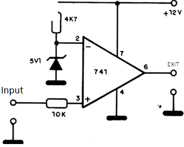
The zener diode fixes the reference at the negative input. Thus, when the input voltage is below the reference voltage, we have a negative difference that will be amplified and will saturate the output at near 0 V. When the input voltage exceeds the reference value, we will have saturation at the positive value closest to the supply voltage. The curve in Figure 9 shows what happens.
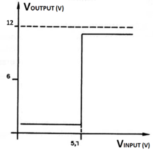
This circuit can be used to send a level 1 to a logic input, or to an indicator circuit, when the input voltage exceeds a certain value.
4. Window Discriminators
By combining the two voltage comparator circuits, we can develop a very interesting configuration called a window discriminator. It receives this name because it only allows a narrow "window" of voltage values to pass through, which are fixed by the reference elements. Thus, for the circuit in Figure 10, the window ranges from 5.1 to 6.2V, at which point the output goes into saturation near zero.
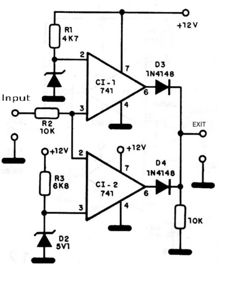
For any other input voltage values, the output voltage will be close to the supply voltage. Diodes D1 and D2 fix the limits or the "width" of the voltage window. The corresponding curve is shown in Figure 11.
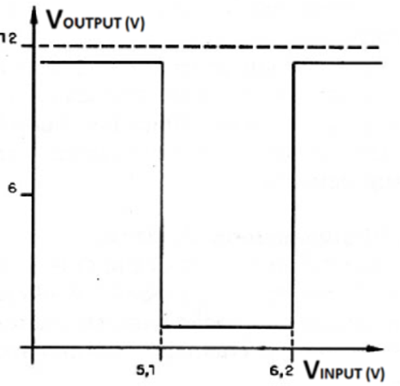
An inverse behavior can be obtained with the circuit in Figure 12.
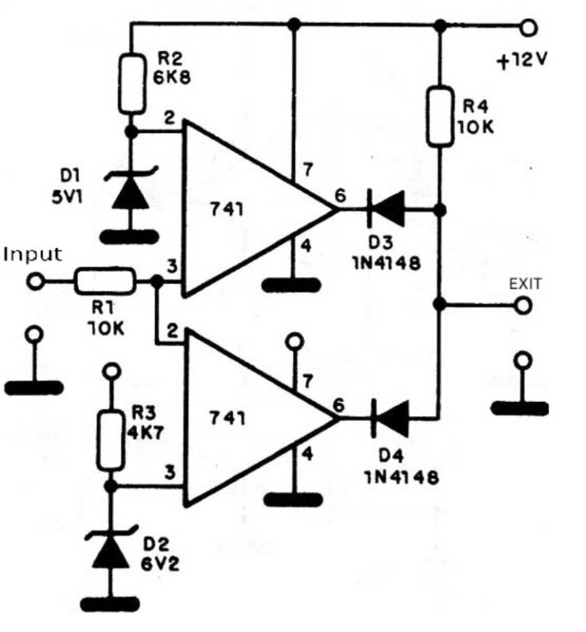
For this circuit, we have a positive output voltage when the input is within the values fixed by the zener diodes. The corresponding curve is shown in Figure 13.
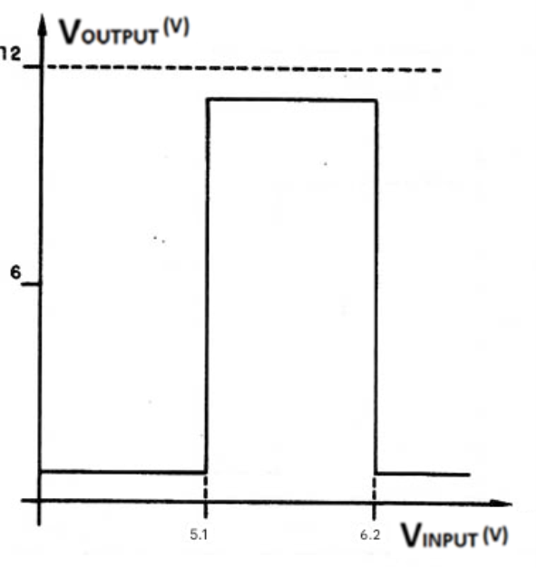
The operation of these circuits is simple: the first comparator maintains the output voltage at a high level until the input exceeds the reference, at which point it drops to zero. The output voltage will remain at zero until the second comparator comes into action. At this moment, its output rises to a high level, remaining so for any value above the reference. We can fix the "window" to any width within the integrated circuit's power supply range simply by choosing the appropriate zener diodes. The input impedance of the circuit is 10 k ohms, which allows direct operation with various types of transducers. Figure 14 shows two relay activation circuits.
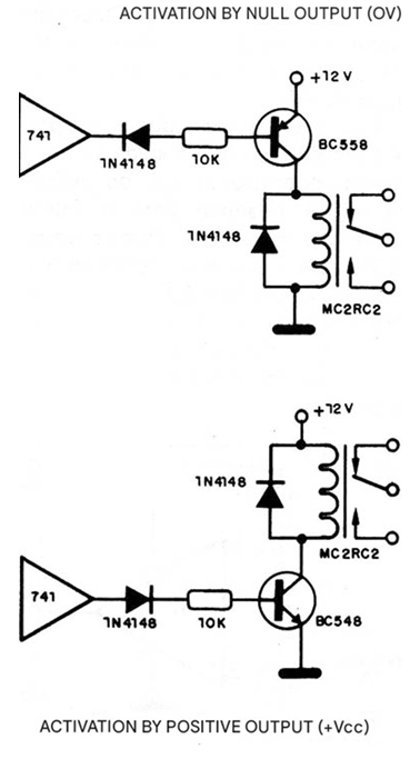
The first circuit activates the relay with high voltage levels, while the second circuit activates the relay with low voltage levels. Note that an important characteristic of these circuits is the lack of need for symmetrical power supplies for the operational amplifiers. Current consumption is quite low for each circuit, with over 90% of the current used to power the relay itself.
REFERENCES
• 110 Operational Amplifier Projects for The Home Constructor - R.M. Marston - 1976.
• Linear Integrated Circuits Data Book – 1976 Fairchild.
• 52 Projects Using IC741 - Rudi & Uwe Redner 1975.


