
DO YOU KNOW ALL THESE POWER SEMICONDUCTORS?
New semiconductor devices make high-power circuit designs simpler, in addition to offering higher efficiency, leading to lower energy consumption and reduced ventilation needs. Several of these devices are still little known to our readers. In this article, we will give an overview of these new devices, comparing their characteristics and providing guidance for design.
ART2235S ART153
The circuits that operate with the most power in modern electronic equipment are their power supplies. In most cases, these power supplies are of the switched-mode type, which require the use of semiconductor devices with special characteristics. These devices must be able to operate with high currents when conducting, withstand high voltages when cut off, and still have sufficiently short switching times so as not to take the device to its intermediate region for a long enough time to cause losses due to heat generation.
The ideal switching device for these applications should have a switching characteristic as shown in Figure 1 with its dashed line, whereas in reality, practical devices have characteristics that correspond to the solid line.
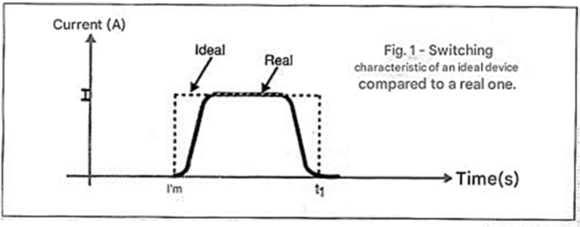
The improvements that traditional semiconductor devices undergo, such as bipolar transistors and thyristors, bring their ideal characteristics ever closer, but at the same time, new devices are being created that prove to be even better in certain situations for their intended applications. Many new devices have been created and are now becoming popular, appearing in switched-mode power supplies, power inverters, solenoid and stepper motor controls, and many other similar applications.
3-LAYER DEVICES
The basic idea for creating new semiconductor devices is the use of 3 layers of semiconductor materials with different structures. These structures will determine the basic characteristics of such devices, which are shown in Figure 2.
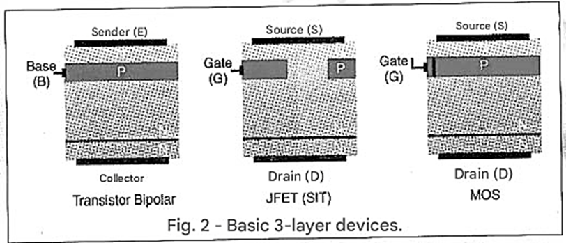
One important characteristic to consider in these structures is that they are vertically oriented with large N-type intermediate regions, allowing the device to operate at high voltages. The three layers of semiconductor materials can be used in various ways, as we can see from the devices cited as examples. In a high-voltage transistor (HVT), the current between the main terminals (emitter and collector) is proportional to the current flowing through the control terminal (base). Its operation is therefore similar to that of any common bipolar transistor.
In the second case, there is an opening in the second layer (P) where the main current can flow, which is then controlled by the voltage applied to the gate terminal. In this case, we have a junction field-effect transistor or JFET. Another name for this device is SIT or Static Induction Transistor, since the intensity of the current between the main electrodes (source and drain) is determined by the intensity of a static field in the channel region through which the current passes.
Finally, we have the third possibility, which consists of placing the control electrode (gate) very close to the P region but without touching it (it is isolated by a layer of insulating material that gives it its name). A voltage on the gate electrode attracts the charge carriers from the N region and thus controls the current flow between the main electrodes. This device is known as a MOS (Metal Oxide Semiconductor) transistor.
Let's analyze these devices separately.
HIGH VOLTAGE TRANSISTOR (HVT)
In this device, a base current controls the current between the collector and the emitter. To work with high power, the base must be made so thin that electrons can flow immediately between the collector and the emitter. Other constructive characteristics must be taken into account in order to achieve good switching speed combined with a large current capacity. A series limitation that occurs in transistors of this type is the phenomenon called "second breakdown" during switching.
The current tends to concentrate in the middle of the emitter region with an increase in its density to the point of causing damage to the device. Devices of this type therefore have a characteristic curve that shows an operating region in which it must be kept in order to avoid this phenomenon. There is then what is called RBSOAR (Reverse Bias Safe Operating Area Region) as shown in Figure 3 where the device can operate safely.
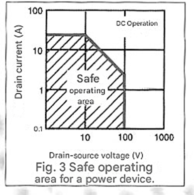
A protection to prevent these characteristics from being violated and damaging the device consists of using a "snubber". This is a network that aims to reduce the rate at which the current intensity increases in the device during switching (i.e., a dV/dt network with an appropriate value). One problem to consider when using a snubber is that its cost is of the same order as that of the transistor itself, although, with inductive loads, their resonance can be used to reduce the rate of voltage rise across the load (dV/dt).
The JFET
An advantage of this device is that there is a pure ohmic resistance between the terminals through which the main current must flow. This means a greater current capacity since there are no junctions to be traversed. Since the main current is controlled by a voltage, the control requires much less power. Since the only function of this control is simply to charge and discharge the diodes formed by the junctions, which can be done very quickly, devices of this type are capable of switching at much higher speeds than their bipolar equivalents. A constructive difficulty for this device lies in the fact that the control electrodes (gates) must be placed in openings close to the source electrodes, and the capacity/speed of the device will depend on their quantity. Thus, the more alternating regions are placed as shown in Figure 4, the greater the speed and current capacity of the device will be.
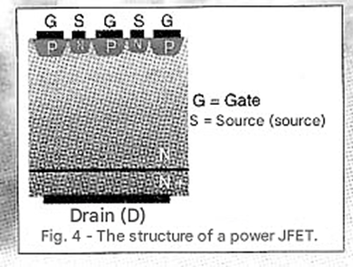
In practice, however, this procedure leads to the need to use high negative voltages to achieve switching. It is common for devices of this type to be specified to have switching with up to 25 volts of negative voltage applied to the gate.
MOS TRANSISTOR
When a positive voltage is applied to the gate electrode, this device is biased in the direction of current conduction between the source and the drain. To obtain a high current capacity, the device must have the structure shown in Figure 4, where the control electrode (gate) is placed practically next to the source electrode in the large N region that characterizes power devices, as discussed in the introduction.
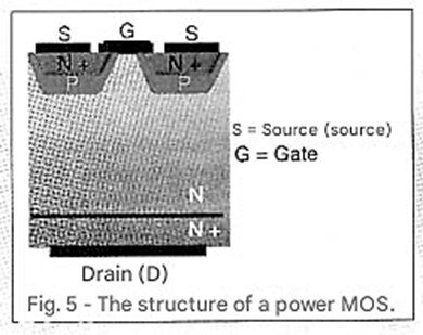
This structure, called planar, allows the fabrication of these devices with large current capacities and characteristics quite similar to JFETs, except that the gate is isolated from the material by a thin layer of metal oxide. Commutation is performed by charging and discharging the capacitor formed by the gate region and the semiconductor material. Since controlling high currents also requires larger areas of this capacitor, there is a charging and discharging current to be considered. The device therefore does not switch only with voltage but also requires a certain current.
It should be noted that this device does not need negative voltages to switch, but applying a negative voltage now it needs to be switched off can make this operation faster. The speed and high current capacity characteristics of this type of device have made it the preferred device in current power switching circuit designs. In addition, the availability of these devices at an affordable cost in a very wide variety of types should be considered.
FOUR-LAYER DEVICES
The devices we have seen are three-layer devices, that is, equivalent to transistors. However, these devices still have certain limitations that can be improved with enhancements to their structure. An important possibility, and one that is used in the creation of new devices, is the adoption of four-layer structures. This implies the creation of a virtual NPN transistor in a three-layer structure that actually corresponds to an NPN transistor, as shown in Figure 6.
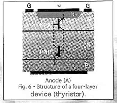
The result is that this transistor can be used to "speed up" the device's operation, serving as a switching element. The very way this additional transistor appears in the structure forms a regenerative circuit that gives the device a new characteristic: latching, as shown in Figure 7.
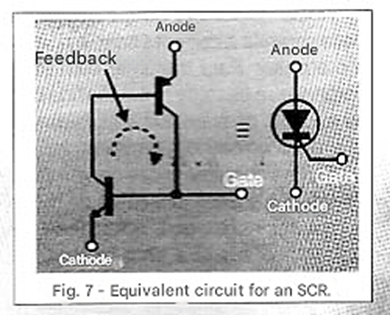
However, it should be considered that in these devices the current has to pass through an additional junction, and this affects both the switching speed and the switching losses themselves. In fact, the voltages that appear between the main electrodes when these devices are fully conducting are much higher than those of the other devices we have seen so far.
THYRISTOR (THY)
An example of a device in this family is the SCR (or Silicon Controlled Rectifier), which basically consists of a high-voltage transistor (HVT) with an additional P-type layer. Thus, it is enough to bias the NPN transistor so that it saturates, and through feedback it saturates the PNP, causing the device to fire, which remains in this state even after the initial switching current disappears.
Although these devices are built with the capacity to switch high currents, their speed is low. This significantly limits their dV/dt. One characteristic of the SCR, which is not always desirable, is that the current between the anode and cathode needs to be reduced to zero momentarily for it to turn off.
The GTO
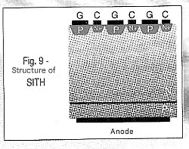
A variation of the SCR that can be turned off by an electrical signal is the GTO or Gate Turn Off Thyristor, which has the structure shown in Figure 9.
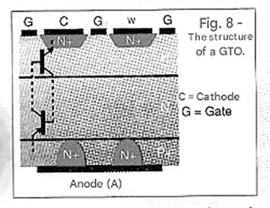
This is a special type of thyristor where the structure has been designed to provide higher switching speeds while also including a feature that allows reducing the gain of one of the feedback transistors by external means. In this way, by applying a negative voltage to the base of the PNP transistor, it is possible to interrupt the feedback current and thus turn off the device. Unfortunately, GTOs are not yet designed to control high power and are therefore indicated for circuits with low power, especially in resonant systems, since the turn-off losses they present are practically zero.
The SITh
The Static Induction Thyristor is a type of thyristor that is also called an FCT (Field Controlled Thyristor) and basically consists of a JFET with an additional P-type layer, as shown in Figure 9.
Unfortunately, obtaining the characteristics that lead to the practical use of this device still presents certain industrial difficulties that make it unavailable on the market.
IGBT
IGBT stands for Insulated Gate Bipolar Transistor. Its structure and symbol are shown in Figure 10, and as we can see, it consists of a "mixture" of a bipolar transistor and a FET; therefore, although it is a component that has an "emitter" and a "collector," the control electrode is not a base but rather a "gate."
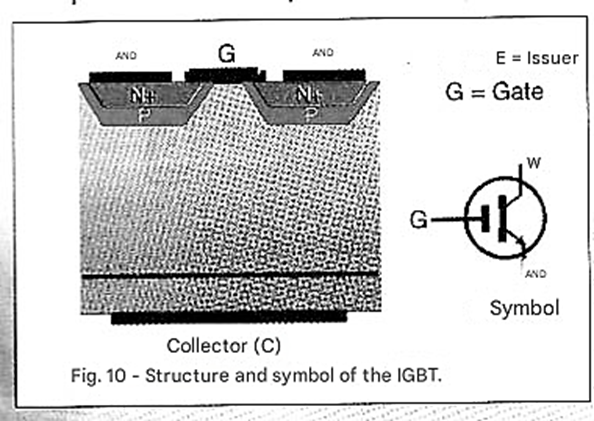
In normal operation, a positive voltage is applied to its anode (A) relative to the cathode (CK). When the gate (G) has zero voltage relative to the cathode, no current flows through the anode as long as the applied voltage is below the limit supported by the component. When the gate voltage reaches a certain minimum value, electrons pass through the n-region of the PNP transistor's base, causing the transistor to be biased towards conduction. This causes holes to be injected from the substrate into the n-region of the device. The excess of electrons and holes modulates the conductivity of the high-conductivity n-region, which rapidly reduces its resistance, causing the device to conduct current intensely.
In normal operation, the shunt resistor (Rs) keeps the emitter current of the NPN transistor very low, and therefore the gain of this transistor is also low. However, for sufficiently intense anode currents, a sufficiently intense current injection can occur in the NPN transistor, causing its alpha gain to increase. In this case, the four-layer device latches, resulting in a loss of control by the MOS gate. In this case, the device must be turned off by decreasing the voltage. Anode current to a value that is below the so-called holding current, as in a typical thyristor. Figure 11 shows the characteristic curves of a MOSFET and an IGBT so that the reader can make comparisons.
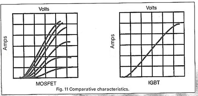
Note that in the IGBT we also have an offset voltage of 0.7 volts from the origin point, from where the curve shows a significant increase in current. This voltage is due precisely to the presence of the junction between the p+ layer and the n- layer of the substrate. The IGBT curve shown in the figure is from a device operating with a gate voltage of 20 volts and shows that the resistance in full conduction, with a current of 20 amperes, is only 0.084 ohms.
This low conduction resistance characteristic, on the order of 0.1 ohm for currents of 20 A, is common to typical devices using 3 x 3 mm chips. Note that these values approximate the characteristics of these devices to those of common power MOSFETs.
CONCLUSION
These new devices (some not so new) should appear with increasing frequency in projects involving the switching of high-power loads such as switched-mode power supplies, solenoid controls, and stepper motors. Technicians and engineers must be able not only to recognize these new devices but also to evaluate their characteristics when they need to carry out new projects, service, or simply look for a replacement.
Bibliography:
• Philips Power Semiconductor Applications
• Power MOSFETs, IGBTs, Ultrafast Rectifiers, Intelligent Discretes, Intelligent Power - Harris Semiconductor


