
The circuit of Figure 1 can be used as receiver for the previous block. Its sensor is a photodiode or phototransistor of any type.
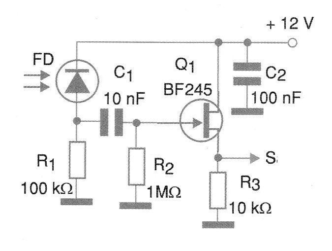
The junction field effect transistor can be of any type. This circuit can work with modulated signals up to a few hundred kilohertz.
Optical features should be used to focus the radiation on the photo sensor and thus obtain greater reach for the link.
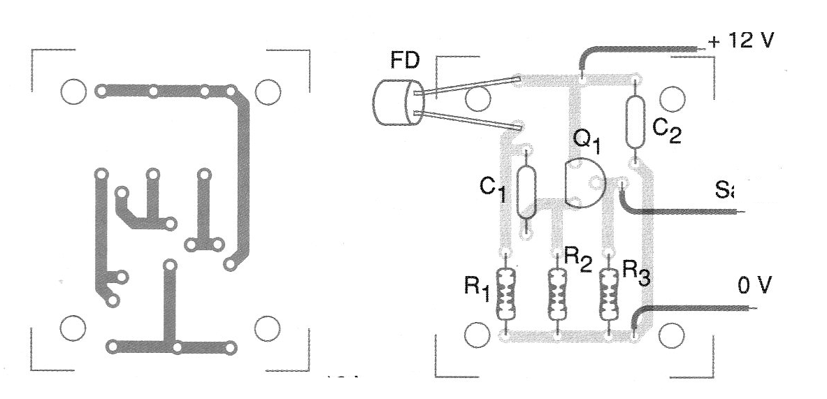
A printed circuit board for the assembly is shown in Figure 2.
MATERIAL LIST
Q1 - BF245 or equivalent - junction FET (JFET)
FD - Photo-diode or photo-transistor
R1 - 100 k ohm x 1/8 W - resistor
R2 - 1 M ohm x 1/8 W - resistor
R3 - 10 k ohm x 1/8 W - resistor
C1 - 10 nF - ceramic or polyester capacitor
C2 - 100 nF - ceramic or polyester capacitor
Miscellaneous:
Printed circuit board, wires, welding, etc.


